 |
 |
| |
|
| |
|
 |
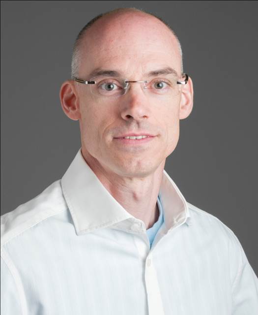
Mr. Chris Bencher
Distinguished Technical Staff
Office of the CTO, Applied Materials Inc.
|
| |
| Profile |
| |
| Education : |
Graduate of Rensselaer and
UC Berkeley with degrees in
Materials Science |
| |
|
Experiences :
|
|
Sidewall Spacer Double Patterning
Advanced Patterning Techniques
SADP, SAQP, DSA Oracle for Semi-Industry |
| |
| Abstract: |
| |
| Multiple Patterning for Immersion Extension and EUV Insertion |
| |
| The lithography roadmap has been challenged in recent years as the projection wavelength scaling stalled relative to feature size since about 2008 corresponding to our 40nm nodes. While the EUV eco‐system makes its closing push on commercialization, design‐integration‐EDA teams have joined together to deploy double patterning techniques for building today’s devices. Three nodes of spacer double patterning having kept memory scaling forward and these memory devices now look to begin insertion of spacer quad patterning. The logic community will benefit from the nodes of experience as spacer double patterning works its way into their FinFET and gate patterning schemes. These efforts are a solid investment because sub‐10nm nodes will require EUV combined with spacer double patterning and for their cut masks. New materials for traditional double exposure techniques also continue to be introduced which simplify process steps and lower cost. Multi‐patterning now, supplemented with EUV in the future, can keep our technologies scaling thru the decade. |

